ITER, a machine that will imitate the sun, will also mimic the sun’s extreme environment: intense heat, strong magnetic fields and radiation. A team at US ITER has been toughening up critical components of ITER’s vacuum system so they can withstand those harsh conditions.
Based in France, the international ITER project is designed to demonstrate the feasibility of fusion power for future carbon-free energy. That power will come from neutrons, one of the energetic byproducts of fusion.
Neutrons, an energetic by-product of the fusion reactions in the ITER device, will not travel in docile single file as they leave the plasma. When running at full power, ITER’s plasma is projected to generate billions and billions of neutrons, each one with 14.1 MeV (mega-electron-volts) of energy. Shielding reduces the neutron flux but neutrons are sub-atomic in size and can scatter and slip between the atoms in concrete. The shielding reduces the number of neutrons to about a million per second per square centimeter outside the protective bioshield.
“Five hundred MW of plasma power will be a sustained radiation environment that the fusion community hasn’t experienced before,” said Kurt Vetter of US ITER, which is managed by the Department of Energy’s Oak Ridge National Laboratory. Vetter leads US ITER’s teams for electron cyclotron and ion cyclotron heating transmission lines and for instrumentation and controls.
Vetter’s group has been designing and building the radiation hardened (“rad hard,” for short) electronics supporting ITER’s vacuum auxiliary system. The electronics will be mounted at 68 locations just outside the bioshield and monitor the vacuum system for leaks and other potential issues.
US ITER engineers aren’t the first to face this problem. Aviation and aerospace engineers need to design around the effects of cosmic radiation in the upper atmosphere and space. On Earth, numerous smaller fusion devices have contended with neutron-yielding plasmas. But radiation from those experiments is orders of magnitude smaller than what ITER will generate.
Neutrons, while short-lived, are a source of both direct and indirect radiation immediately around the tokamak. ITER will restrict access to this area and further protects staff and instrumentation with a 3.2-meter-thick concrete bioshield. But some of these neutrons, and the gamma rays they spawn when interacting with the cooling water around the tokamak, can still threaten nearby equipment.
Consequently, sensitive components need to be rad hard — designed and built with years of radiation exposure in mind. That includes the vacuum auxiliary system components being delivered by US ITER.
The vacuum system ensures ITER has the clean, low-pressure environment needed to sustain plasma efficiently in the tokamak. Vetter’s team has been working to protect the vacuum system’s most sensitive components, including 1,000 piezo pilot valves being fabricated by Dynamic Structures & Materials, LLC in Franklin, Tenn. and 4,000 piezo pressure sensors being developed by PMC Engineering in Danbury, Conn. Prototypes of both components are expected later this year.
The team’s approach is informed by a study led by Katherine Royston of ORNL’s Nuclear Energy and Fuel Cycle Division that analyzed ITER radiation transport and shielding. Her reports demonstrated that the predicted flux — neutrons per square centimeter per second — was far beyond what normal electronics could tolerate. Since there was no room for additional shielding, the team needed to find a way to toughen up the electronics.
Vetter had previously worked on rad-hard electronics for CERN’s ATLAS experiment and was familiar with CERN’s expertise in this area. To mitigate events where a stray particle hits a computer chip, CERN developed a special kind of integrated circuit (or ASIC, for application specific integrated circuit), so single event upsets can be filtered out as noise.
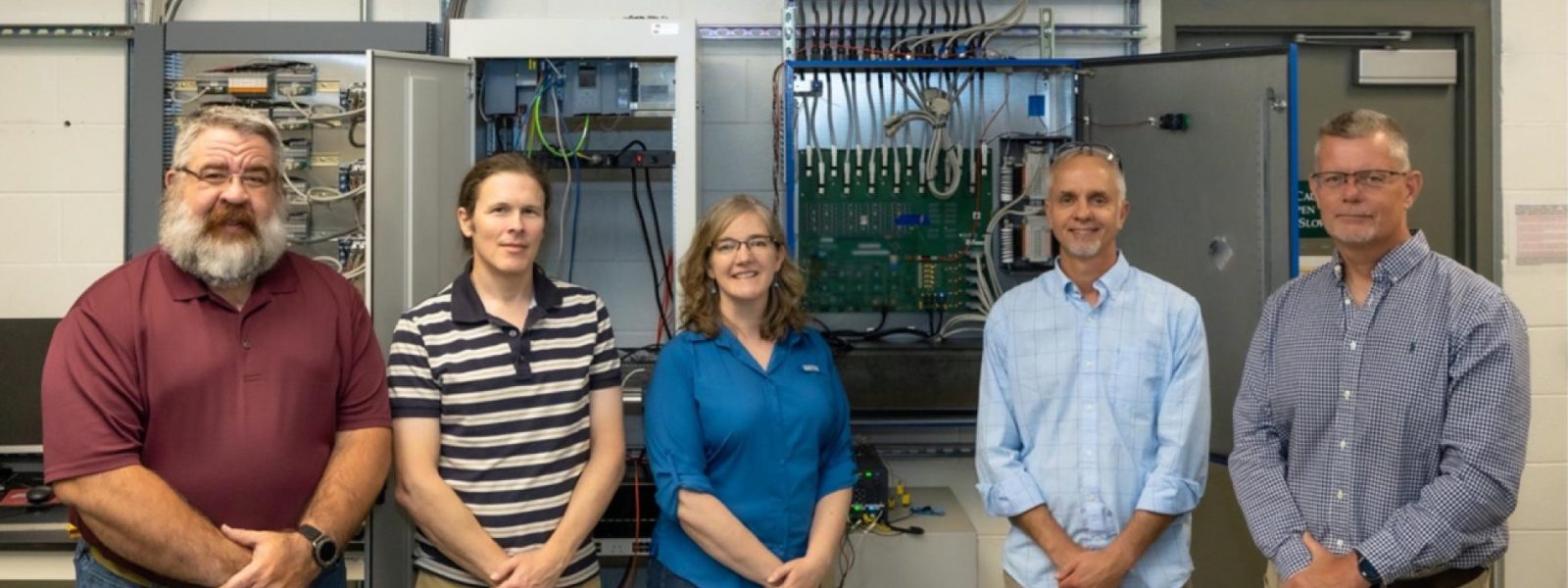
The team leveraged that groundwork in their electronics design. The CERN ASIC form the backbone of the Front End Acquisition and Control (FEAC) board, which digitizes sensor data and provides readback and control. The FEAC will interface with an Analog Front End (AFE) board, which controls the valves and the signal condition of the pressure sensors. These two rad-hard boards will connect via rad-hard fiber optics to a third component, the Profinet digital interface, to be located in a shielded area. A power management module completes the array.
Another team from ORNL’s Electrification and Energy Infrastructures Division built these four electronic boards and is completing testing at ORNL. After a final design review this summer, the team will prepare for fabrication: One thousand of the CERN integrated circuits are already on hand, waiting to be assembled into the FEAC boards.
Vetter said collaborations with CERN, the ITER Organization and numerous ORNL colleagues have been key to the progress.
“It is very exciting to be able to contribute to such an important and challenging project,” Vetter said.
The work is supported by DOE’s Office of Science. UT-Battelle manages ORNL for the Department of Energy’s Office of Science, the single largest supporter of basic research in the physical sciences in the United States. The Office of Science is working to address some of the most pressing challenges of our time. For more information, please visit energy.gov/science.